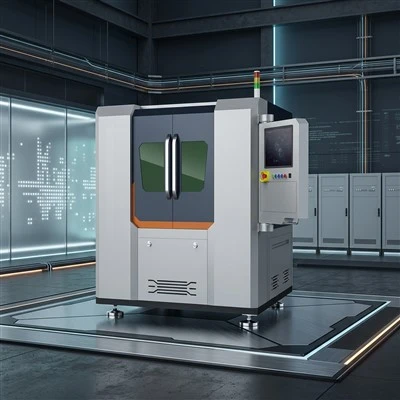
Key Advantages
- ±5μm CCD visual positioning system for ultra-precise alignment
- Micro-crack-free ceramic cutting through proprietary pulse control
- Selective copper etching without damaging underlying ceramic
- Micro-via array machining for 0.1–0.5mm heat dissipation and connection holes
- 3D contour machining for stepped and curved power module structures
Machine Features
-
Precise Layered Machining
- Intelligent laser parameter control for precise cutting depth
- Clean separation of ceramic and copper layers
- Heat-affected zone (HAZ) minimized to <30 μm
- Machining accuracy ±0.01 mm ensures consistent alignment with terminal configurations
-
Crack-Free Cutting
Proprietary pulse control technology prevents micro-cracks in ceramic layers
-
Selective Etching
Precise removal of copper in designated areas without affecting the ceramic substrate
-
Micro-Via Array Machining
Drilling holes for thermal management and electrical connections
-
3D Contour Machining
Supports stepped and curved shapes of power module assemblie
Technical Data
|
Item |
Parameter |
|
Laser wavelength |
1060-1080nm |
|
Laser output power |
150W(optional) |
|
Max.cutting range |
300*300mm |
|
Cutting thickness |
0.2-2mm(Depending on material) |
|
Precision of repeated positioning of X/Y axis |
±3µm |
|
CCD visual positioning system |
Positioning accuracy ±5µm |
|
Processing speed |
0-2500mm/min |
|
Maximum acceleration |
1.0G |
|
Machining accuracy |
±0.01-0.02mm |
|
Worktable precision |
≦0.015mm |
|
Transmission mode |
linear motor +0.1µm grating ruler |
|
Whole machine power (no fan) |
≦6KW |
|
Total weight of the whole machine |
About 1700KG |
|
External dimension(length*width*height) |
1400*1500*1800mm (For reference) |
Application Scenarios
- IGBT Power Modules: Precision cutting of ceramic substrates and copper layer patterning
- SiC / GaN Semiconductor Modules: Separate processing of signal and power terminals
- Power Module Post-Packaging:Surface patterning, micro-drilling, and alignment for assembly
- Photovoltaic inverters, industrial frequency converters, and other high-end power electronic devices.
OEM & Customization Options
- Adjustable laser power and XY platform configuration for various DBC substrate types
- Customizable software for selective copper etching and ceramic layer processing
- Tailored solutions for high-precision multi-terminal module manufacturing
Quality Control
- CCD visual alignment for ±5μm positioning accuracy
- Micro-crack-free ceramic processing
- Real-time monitoring and defect detection
- Full-process traceability to ensure high yield and reliability
After-Sales Service
- On-site or remote installation and commissioning
- Operator training and workflow optimization
- Technical support and troubleshooting
- Spare parts availability and long-term maintenance
FAQ
Q1: Can the machine process multi-layer DBC substrates for SiC/GaN modules?
A1: Yes, it supports layered machining with precise separation of ceramic and copper layers.
Q2: What is the positioning accuracy?
A2: XY positioning ±3μm and CCD visual positioning ±5μm.
Q3: Does it support micro-via drilling?
A3: Yes, 0.1–0.5mm diameter micro-vias for thermal management and electrical connections.
Q4: Can the machine etch copper selectively without damaging ceramic?
A4: Absolutely, the laser can precisely remove copper in designated areas while preserving the ceramic substrate.
Hot Tags: dbc laser drilling machine, China dbc laser drilling machine manufacturers, suppliers, factory, PCB Substrate Laser Cutting Machine, aln laser cutting machine, DBC Laser Drilling Machine, 5G Packaging Laser Drilling Machine