Precision Laser Processing for PCB and Electronic Substrates
YCLaser provides customized laser cutting systems for PCB substrates, FPC, HDI boards, metal substrates and ceramic substrates. Our systems support precision cutting, depaneling, slotting and drilling with different laser sources selected according to material, thickness, feature size and edge-quality requirements.
From prototype development to production applications, we provide sample testing and process evaluation to help customers select the appropriate laser configuration before purchasing equipment.
Request a Sample Test
-
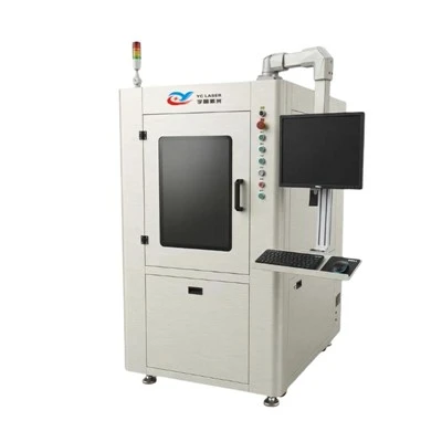
![PCB Substrate Precision Laser Cutting Machine]() PCB Substrate Precision Laser Cutting MachineYC-GJMPCB is specifically designed for precise cutting and shaping of PCB rigid boards, FPC flexible boards, HDI boards, ceramic substrates, and composite substrates. Based on customer-provided
-
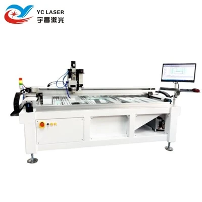
![PCB Copper Laser Cutting Machine]() PCB Copper Laser Cutting MachineThis equipment utilizes advanced fiber lasers for efficient cutting and grooving of metal substrates such as copper and aluminum substrates, providing a one-stop precision machining solution for
-
![PCB Ceramic Laser Cutting Machine]() PCB Ceramic Laser Cutting MachineThis equipment is primarily used for high-precision cutting of ceramic substrates. It's an economical precision laser cutting solution optimized for the large-scale production needs of PCB ceramic


PCB Materials We Process
Different PCB structures require different laser sources and processing strategies. Our PCB laser cutting machines can be configured for a range of rigid, flexible, metal and ceramic substrates.
Rigid PCB
- FR4 substrates
- Rigid PCB boards
- HDI boards
- Multilayer PCB
- Composite substrates
Flexible PCB
- FPC
- Flexible circuits
- Thin electronic substrates
- Flexible copper structures
Metal Substrates
- Copper substrates
- Aluminum substrates
- Metal-core PCB
- Copper and aluminum layers
Ceramic Substrates
- Alumina (Al₂O₃)
- Aluminum Nitride (AlN)
- DBC
- AMB
- LTCC / HTCC
For materials with different compositions or thicknesses, laser parameters are developed through sample testing rather than relying on a single standard configuration.

PCB Laser Machine Market and Industry Applications
The PCB laser machine market is developing alongside the growing demand for precision electronic manufacturing, power electronics, semiconductor packaging and compact electronic devices. As PCB designs become smaller and more complex, manufacturers increasingly require flexible processing solutions for cutting, depaneling, drilling and precision substrate processing.
Laser processing is used across different segments of the PCB industry, from conventional rigid boards and FPC to HDI, copper substrates and advanced ceramic substrates.
Key application areas include:
- Consumer Electronics — compact PCB and FPC processing
- Automotive Electronics — precision electronic components and power electronics
- 5G & RF Electronics — high-frequency and ceramic substrates
- Power Electronics — copper, aluminum, DBC and AMB substrates
- Semiconductor Packaging — precision ceramic and electronic substrates
- LED & Thermal Management — alumina and aluminum nitride substrates
The PCB laser machine market also covers different laser technologies, including fiber laser, UV nanosecond laser and UV picosecond laser. The appropriate system depends on substrate material, thickness, copper content, feature size, production volume and required processing quality.
For this reason, machine selection should be based on the actual PCB material and application rather than on laser power alone.
PCB Laser Processing Applications
A PCB laser cutting machine can perform several non-contact processes on electronic substrates.
| Process | Typical Applications |
| Laser Cutting | PCB contour cutting and precision profiling |
| Laser Depaneling | Separating individual boards from panels |
| Laser Slotting | Slots, grooves and openings |
| Laser Drilling | Functional holes and precision holes |
| Fine Cutting | Thin and small electronic substrates |
| Ceramic Substrate Cutting | Alumina, AlN, DBC and AMB substrates |
Compared with mechanical routing or blade cutting, laser processing eliminates direct tool contact with the substrate. This can help reduce mechanical stress and is particularly useful for delicate circuits, thin substrates and complex contours.
PCB Laser Machine Advantages for Precision Processing
Non-Contact Processing
1
>>
High-Precision Processing
2
>>
Flexible Production
3
>>
Vision Alignment
4
>>
Multi-Material Capability
5
Non-Contact Processing: Laser cutting does not require a mechanical cutting tool to contact the PCB. This helps reduce vibration and mechanical stress during depaneling and contour cutting.
High-Precision Processing: Precision motion systems, laser scanning and CCD vision positioning can be combined to process small features and complex PCB geometries.
Flexible Production: Laser processing is software-controlled, allowing cutting patterns to be changed without manufacturing a dedicated mechanical die or cutting tool.
Vision Alignment: CCD vision systems can identify fiducial marks and compensate for positioning deviations, helping maintain consistent cutting accuracy during production.
Multi-Material Capability: Different laser sources and power configurations can be selected for FR4, FPC, copper, aluminum and ceramic substrates instead of using one laser configuration for every material.
Laser selection depends on the PCB material, thickness, metal content, feature size and required edge quality.
Get a Machine Recommendation
Fiber Laser
For Metal-Rich and Thicker Substrates
Suitable applications include:
- Copper substrates
- Aluminum substrates
- Metal-core PCB
- Thicker metal-containing boards
Fiber lasers provide high processing efficiency for metal substrates and can be configured for cutting and grooving applications.
UV Nanosecond Laser
For Thin and Precision Substrates
Suitable for applications requiring finer processing and controlled thermal effects, including:
- Thin PCB
- FPC
- HDI
- Ceramic substrates
- Small precision features
UV laser processing can be particularly useful where material sensitivity and edge quality are important.
UV Picosecond Laser
For Fine Micro-Features
For applications requiring tighter control of thermal effects and smaller features, UV picosecond lasers can be considered for:
- Fine lines
- Small slots
- Micro features
- Precision electronic substrates
PCB Laser Cutting Applications

Power Electronics
Laser processing can be used for ceramic and metal substrates used in power modules, including DBC and AMB substrates.
5G & RF Electronics
Precision cutting and drilling are suitable for RF substrates, antenna-related components and ceramic electronic structures.
Automotive Electronics
PCB and substrate processing can support electronic components used in automotive control systems, sensors and new-energy applications.
Consumer Electronics
Laser processing is suitable for compact PCB, FPC and precision electronic components where flexible geometries and small features are required.
Semiconductor Packaging
Ceramic and other precision substrates can be processed for packaging-related applications requiring controlled dimensions and complex contours.
LED & Electronic Substrates
Alumina and aluminum nitride substrates can be processed for LED, thermal-management and other electronic applications.
PCB Laser Machine Solutions for Your Application
As the PCB laser machine market continues to move toward smaller features, more complex substrates and higher processing requirements, choosing the right laser system is becoming increasingly important.
Send us your material, thickness, drawing and samples. Our engineers can evaluate the application, perform sample testing and recommend a suitable PCB laser machine configuration.

1. Send Your Samples
Provide your PCB, FPC, copper, aluminum or ceramic substrate samples.
2. Material Evaluation
Our engineers evaluate the material structure, thickness and processing requirements.
3. Laser Selection
Fiber, UV or UV picosecond processing can be evaluated according to the application.
4. Sample Cutting
We develop suitable processing parameters and perform sample cutting.
5. Result Evaluation
Cutting quality, dimensional accuracy, edge condition and other requirements are evaluated.
6. Machine Recommendation
Based on the test results, we recommend a suitable machine configuration.
Request Free PCB Sample Testing
FAQ
Q: What positioning accuracy can the PCB laser cutting machine achieve?
A: For the standard precision configuration, the X/Y repeated positioning accuracy is up to ±5 μm, while the CCD visual positioning accuracy can reach ±5 μm. Actual cutting tolerance depends on material, thickness, geometry, laser source, and process parameters.
Q: What motion system is used for precision PCB processing?
A: The machine uses an imported linear motor with a 0.5 μm grating scale for precision position feedback. This closed-loop motion architecture helps maintain positioning stability during high-precision cutting and contour processing.
Q: What is the working area and processing speed?
A: A typical configuration provides a 600 × 600 mm working area with processing speeds of up to 500 mm/s. The actual cutting speed depends on PCB material, thickness, geometry, laser power, and required edge quality. (Customizable dimensions)
Q: How accurate is the machine's worktable?
A: The worktable precision is specified at ≤0.015 mm for the referenced configuration. Combined with linear-motor positioning, grating-scale feedback, and CCD alignment, the platform is designed for precision PCB and substrate processing.
Q: What determines the final cutting tolerance and edge quality?
A: Final results depend on more than the machine's nominal positioning accuracy. Key factors include material type, substrate thickness, laser wavelength, laser power, beam quality, optical spot size, cutting speed, focus position, workholding, and processing strategy.
For this reason, machine specifications should be evaluated together with actual sample results.
Q: Can the machine be tested with our PCB samples before purchase?
A: Yes. We recommend sample testing for demanding PCB and substrate applications. Customers can provide samples or drawings, and our engineers can evaluate the material, thickness, geometry, required accuracy, and edge quality before recommending a suitable laser configuration.
We are one of the most professional pcb laser cutting machine manufacturers and suppliers in China, also support customized service. Be free to buy industrial pcb laser cutting machine for sale here and get quotation from our factory. For price consultation, contact us.