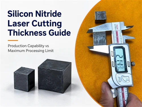
Due to the excellent strength, fracture toughness, thermal stability and wear resistance of silicon nitride ceramic, it can survive harsh operating environments that traditional ceramics and metals fail to endure.
However, these advantages also create significant challenges during laser cutting. As silicon nitride thickness increases, thermal stress control, energy penetration, processing efficiency, and edge quality become increasingly difficult to manage.
Therefore, when evaluating a silicon nitride laser cutting machine, the maximum cutting thickness is not the only important specification. The real industrial capability depends on:
>> Processing stability
>> Production yield
>> Cutting efficiency
>> Long-term reliability
Why Thick Silicon Nitride Is Difficult to Cut
Silicon nitride is a typical hard and brittle ceramic material. Unlike metals, it cannot absorb mechanical stress through plastic deformation. Excessive thermal or mechanical impact may cause:
>> Edge chipping
>> Internal micro cracks
>> Surface defects
>> Reduced component reliability
When processing thicker Si₃N₄ ceramics, several technical challenges become more significant.
1. Increasing Thermal Stress
During laser cutting, heat is generated inside the ceramic material. For thicker components, heat accumulation and temperature differences between the surface and internal layers can increase thermal stress.
Without proper thermal management, thick silicon nitride parts may develop hidden cracks that are difficult to detect during initial inspection.
2. Reduced Energy Efficiency During Deep Cutting
Silicon nitride ceramics have complex optical and thermal properties. When cutting thick materials, laser energy must penetrate deeper into the material.
This usually requires:
>> Multiple scanning passes
>> Optimized pulse energy control
>> Careful heat dissipation management
Without proper process optimization, defects such as rough cutting surfaces and edge damage may occur.
3. Lower Processing Efficiency
As thickness increases, cutting time does not increase linearly.
Thick silicon nitride requires additional processing steps, including:
>> Multi-pass cutting
>> Cooling intervals
>> Parameter adjustment
>> Path optimization
Therefore, a thickness that can be achieved in laboratory testing may not always be suitable for continuous industrial production.
Silicon Nitride Laser Cutting Thickness Classification
Based on practical industrial processing requirements, silicon nitride laser cutting thickness can generally be divided into three ranges.
| Thickness Range | Typical Applications | Processing Status |
| 0.2–3mm | AMB substrates, power electronics ceramics, precision components | High-volume production |
| 4–8mm | Mechanical parts, ceramic rings, structural components | Stable production |
| 9–11mm | Thick ceramic structures, aerospace parts, industrial components | Practical production range |
| 12–21mm | Large structural ceramics and special applications | Prototype / special processing |
Stable Production Range: 0.2–11mm Silicon Nitride Processing
For industrial applications, silicon nitride components within the 0.2–11mm thickness range represent the most practical production area.
This range covers:
>> Thin ceramic substrates for power electronics
>> Medium-thickness mechanical components
>> Thick structural ceramic parts
For thicknesses up to approximately 11mm, a properly optimized ceramic laser cutting system can achieve a balance between:
>> Cutting speed
>> Edge quality
>> Processing stability
>> Production cost
YCLaser focuses on this practical industrial range by optimizing laser parameters, motion control systems, and thermal management strategies specifically for advanced ceramics.
12–21mm Silicon Nitride: Customized Processing for Special Applications
For silicon nitride components above 12mm thickness, laser processing becomes more challenging due to increased thermal stress, longer processing cycles, and stricter parameter control requirements.
These thickness ranges are generally considered suitable for:
>> Prototype development
>> Process verification
>> Customized ceramic components
rather than standard high-volume production.
Through continuous process optimization, YCLaser has successfully performed laser cutting tests on 21mm thick silicon nitride ceramic samples. Under customized processing conditions, the cutting performance and edge quality achieved satisfactory results.
However, ultra-thick Si₃N₄ processing requires comprehensive evaluation of:
>> Material grade and density
>> Component geometry
>> Required edge quality
>> Production volume
>> Cost efficiency
Therefore, YCLaser does not simply define maximum thickness by a single test result. Instead, we focus on providing practical processing solutions based on each customer's application requirements.
For special silicon nitride ceramic cutting projects, including thick-section components beyond standard production ranges, customers are welcome to contact YCLaser for technical evaluation and customized laser processing solutions.