As electronic packaging technologies continue to evolve, high-precision alumina ceramic laser cutting has become essential for manufacturing LED packages, power modules, RF components, semiconductor substrates, and other high-reliability electronic devices. Proper laser processing standards help ensure dimensional accuracy while minimizing chipping, heat-affected zones (HAZ), and microcracks.
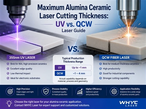
This guide summarizes recommended processing specifications for 96% and 99% sintered alumina (Al₂O₃) ceramic substrates with typical thicknesses ranging from 0.2 mm to 1.2 mm, using a 355 nm UV nanosecond laser cutting machine.
1. Applicable Materials & Equipment
Applicable Materials
---- 96% Alumina Ceramic
---- 99% Alumina Ceramic
---- Typical substrate thickness: 0.2–1.2 mm
Recommended Equipment
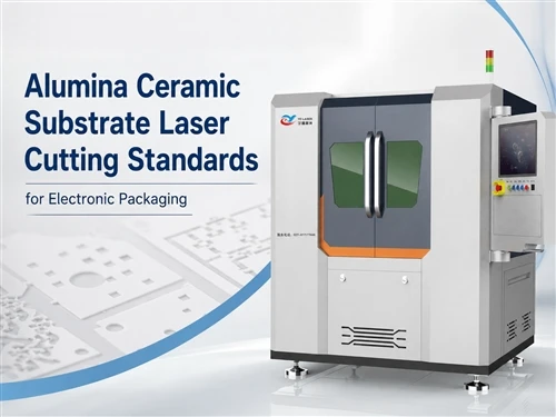
---- 355 nm UV Nanosecond Laser Cutting Machine
---- Adjustable repetition frequency: 80–150 kHz, optimized according to material thickness and cutting requirements.
2. Recommended Processing Practices
To minimize thermal damage and edge chipping, the following practices are recommended:
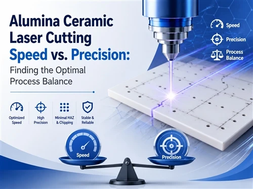
---- Multi-pass layer-by-layer cutting instead of single-pass full-depth cutting
---- Automatic corner deceleration with radius transitions
---- Dual-channel 4–5 bar dry compressed air assist
---- Vacuum worktable maintained at 25 ± 1°C
---- UV-resistant protective film during processing
3. Dimensional Accuracy
Typical Dimensional Tolerance
Under stable processing conditions:
---- ±8–15 μm
Process optimization and proper fixturing can further improve consistency for demanding electronic packaging applications.
Geometric Tolerances
Recommended specifications include:
---- Sidewall perpendicularity ≥ 89.9°
---- Flatness ≤ 0.02 mm / 50 mm
---- Internal corners with minimum R0.05 mm unless otherwise specified
---- Lead-in/lead-out paths recommended for closed contours to reduce stress concentration
Kerf Width Consistency
Typical UV laser kerf width:
---- 15–30 μm
Uniform kerf width helps maintain dimensional consistency across the entire workpiece.
4. Edge Quality Requirements
Edge Chipping
Recommended limits:
---- General edges: ≤ 10 μm
---- Corner regions: ≤ 15 μm
Continuous chipping and radial cracks should be avoided.
Recast Layer & Discoloration
High-quality cutting should exhibit:
---- No visible carbonization
---- Minimal recast layer
---- Uniform edge color
---- No significant residue after cleaning
Surface Roughness
Recommended:
---- Ra ≤ 2 μm
Cut surfaces should be free from burrs, slag accumulation, and adhered particles.
5. Heat-Affected Zone (HAZ) & Crack Control
Recommended HAZ:
---- Typically below 10 μm
For high-reliability applications, further optimization is recommended.
The finished parts should be inspected to ensure:
---- No through cracks
---- No radial cracks
---- No obvious subsurface microcracks
Metallographic microscopy, SEM inspection, or other non-destructive evaluation methods may be adopted according to customer requirements.
6. Micro-Hole Processing
For ceramic substrates with precision holes:
Recommended process:
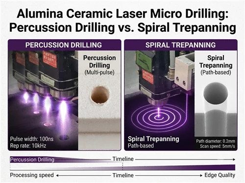
---- Spiral progressive laser drilling
---- Avoid single-pass drilling
Typical capability:
---- Minimum hole diameter: approximately 0.15 mm
---- Positional accuracy up to ±5 μm (depending on material and process)
---- Smooth hole walls
---- Flat blind-slot bottoms without cracks
Why Choose YCLaser?
Achieving high-quality alumina ceramic laser cutting requires far more than a 355 nm UV laser source. It depends on machine stability, precision motion control, optimized process parameters, and extensive experience in advanced ceramic machining.
WHYC Laser specializes in precision laser micromachining solutions for advanced ceramics, offering integrated solutions for laser cutting, drilling, grooving, scribing, and customized ceramic processing.
Our systems are widely used for:
---- Alumina (Al₂O₃)
---- Aluminum Nitride (AlN)
---- Zirconia (ZrO₂)
---- Silicon Nitride (Si₃N₄)
---- Silicon Carbide (SiC)
---- Quartz, Sapphire, and other advanced ceramic materials
Whether your application involves electronic packaging, DBC/AMB substrates, power electronics, semiconductor manufacturing, or medical ceramics, our engineering team can provide customized laser processing solutions tailored to your production requirements.
Contact YCLaser today to request free sample processing, discuss your application, or receive a customized ceramic laser machining solution from our experts.