Silicon nitride (Si₃N₄) is one of the most advanced engineering ceramics available today. Thanks to its high strength, excellent wear resistance, thermal shock resistance, and chemical stability, it is widely used in semiconductor packaging, power electronics, ceramic bearings, aerospace components, automotive parts, and precision industrial equipment.
However, these outstanding properties also make Si₃N₄ one of the most difficult ceramics to process by laser. Manufacturers often face challenges such as edge chipping, micro-cracks, inconsistent cutting quality, and delayed cracking after machining. Compared with alumina (Al₂O₃), aluminum nitride (AlN), and silicon carbide (SiC), silicon nitride requires much tighter control of laser energy and processing conditions.
This article explains why Si₃N₄ is particularly challenging to laser cut and what factors should be considered before selecting a Silicon Nitride Laser Cutting Machine.
1. Extremely High Hardness Increases Crack Sensitivity
Silicon nitride has a typical Vickers hardness of 1500–1800 HV, making it one of the hardest structural ceramics.
Unlike metals, Si₃N₄ has almost no plastic deformation capability. During laser cutting, localized thermal expansion cannot be released through material deformation, causing stress to concentrate near the cutting edge.
As a result, excessive thermal input may lead to:
›››Edge chipping
›››Corner fractures
›››Surface micro-cracks
›››Crack propagation
For precision components, maintaining stable laser energy is far more important than simply increasing cutting speed.
2. Localized Thermal Stress Is Difficult to Control
Laser cutting produces extremely concentrated heat within a very small area.
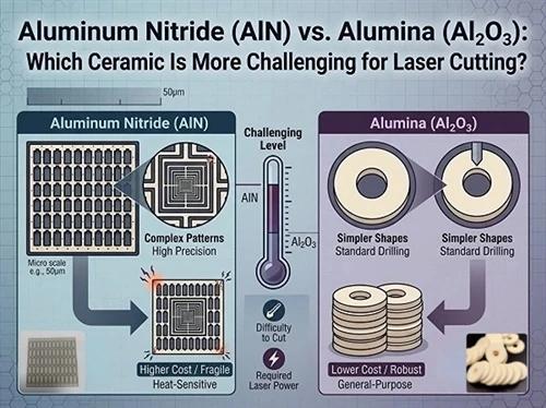
Compared with aluminum nitride, which quickly transfers heat away from the cutting zone, silicon nitride retains more thermal energy around the laser path. The resulting temperature gradient creates high residual stress inside the material.
Typical defects include:
›››Edge cracking
›››Hidden internal cracks
›››Larger heat-affected zones (HAZ)
›››Reduced mechanical reliability
For this reason, thermal management is one of the biggest challenges in Si₃N₄ laser processing.
3. Infrared Lasers Have Lower Processing Efficiency
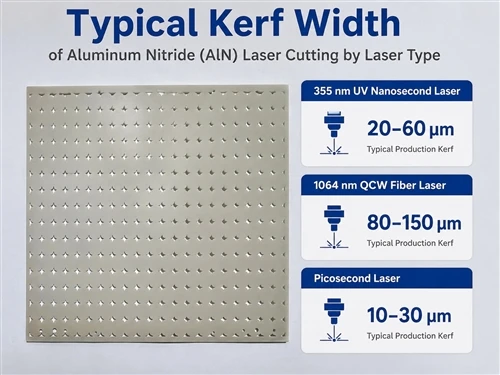
Silicon nitride absorbs 355 nm UV lasers much more efficiently than conventional 1064 nm infrared fiber lasers.
With infrared lasers, more energy is reflected instead of being absorbed by the material. Operators often compensate by increasing laser power or reducing cutting speed, which also increases heat accumulation.
This may result in:
›››Wider kerf widths
›››More thermal damage
›››Lower dimensional consistency
›››Greater risk of micro-cracking
For high-precision applications, UV laser processing generally provides better stability and edge quality.
4. Oxidation Can Reduce Edge Quality
Laser processing generates extremely high localized temperatures.
Without proper shielding gas, silicon nitride may oxidize during cutting, affecting:
›››Edge appearance
›››Surface cleanliness
›››Mechanical strength
›››Electrical insulation for electronic components
High-purity nitrogen is therefore commonly used during precision laser cutting to suppress oxidation and improve surface quality.
5. Residual Stress May Cause Delayed Cracking
One characteristic that makes silicon nitride particularly challenging is delayed cracking.
A component may appear defect-free immediately after cutting, yet microscopic residual stresses remain inside the material. During storage or thermal cycling, these stresses may gradually develop into visible cracks hours or even days later.
For semiconductor substrates and high-reliability ceramic components, minimizing residual stress is just as important as achieving clean cutting edges.
Comparison with Other Engineering Ceramics
| Material | Processing Difficulty | Primary Challenge |
| Alumina (Al₂O₃) | Low–Medium | Moderate thermal damage |
| Aluminum Nitride (AlN) | Medium | High thermal conductivity and oxidation control |
| Silicon Carbide (SiC) | Medium–High | High hardness |
| Silicon Nitride (Si₃N₄) | Very High | Thermal stress, crack sensitivity, residual stress |
Compared with other advanced ceramics, silicon nitride generally requires the most precise control of laser parameters to achieve stable production quality.
Why Process Control Matters More Than Laser Power
Many buyers focus primarily on laser power when selecting equipment. In reality, successful Si₃N₄ processing depends much more on overall process control.
Critical factors include:
›››Appropriate laser wavelength
›››Pulse energy stability
›››Multi-pass cutting strategy
›››Motion platform accuracy
›››Shielding gas protection
›››Thermal management
A well-optimized YCLASER Silicon Nitride Laser Cutting Machine can often achieve higher yield and better edge quality than a higher-power system with poor process control.
Typical Applications
High-quality laser cutting is widely required for:
›››Semiconductor ceramic substrates
›››Power module substrates
›››Ceramic bearings
›››Mechanical seal rings
›››Aerospace structural ceramics
›››Precision industrial components
›››Automotive ceramic parts
These applications typically prioritize crack-free processing, dimensional accuracy, and long-term reliability over maximum cutting speed.
Conclusion
Achieving stable, high-quality cutting therefore requires much more than selecting a high-power laser. Success depends on choosing the appropriate laser wavelength, optimizing process parameters, minimizing thermal input, and maintaining excellent motion accuracy throughout production.
In our next article, How to Laser Cut Silicon Nitride (Si₃N₄): Equipment, Process and Buying Guide, we'll discuss the best laser sources, recommended machine configurations, cutting strategies, and practical purchasing considerations for different Si₃N₄ applications.
Looking for a Professional Silicon Nitride Laser Cutting Machine?
YCLaser specializes in precision laser processing solutions for advanced ceramics, including Si₃N₄, AlN, Al₂O₃, SiC, zirconia, wafers, DBC, and DPC substrates.
Our Silicon Nitride Laser Cutting Machines support material thicknesses up to 11 mm and are available with customized configurations for semiconductor substrates, power electronics, and industrial ceramic components.
Contact us today for free sample testing and process evaluation to find the right laser solution for your application.