Introduction
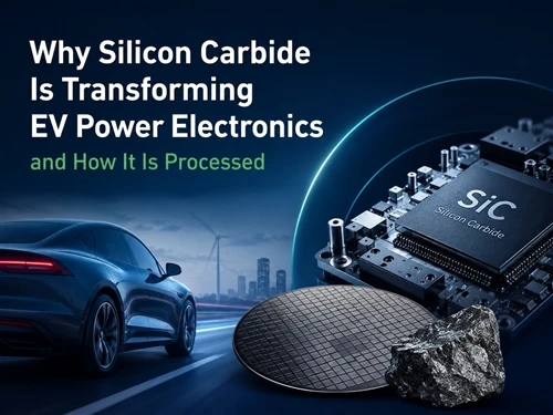
Silicon carbide (SiC) has become one of the most important advanced materials for power electronics, electric vehicles (EVs), renewable energy systems, aerospace, and semiconductor manufacturing. Thanks to its exceptional hardness, high thermal conductivity, chemical stability, and wide bandgap properties, SiC enables devices to operate under higher voltages, temperatures, and switching frequencies than conventional silicon.
However, these same properties also make silicon carbide one of the most challenging materials to machine. Conventional mechanical methods often suffer from severe tool wear, edge chipping, micro-cracks, and low machining efficiency, especially when processing high-precision ceramic components or semiconductor wafers.
As a result, laser processing has become a key manufacturing technology throughout the silicon carbide value chain. From crystal preparation and wafer manufacturing to chip packaging and precision ceramic machining, laser technology enables higher precision, lower material loss, and greater production efficiency than many traditional machining methods.
In this guide, we'll explore the major laser processing technologies used for silicon carbide, their typical applications, and the advantages they offer in modern manufacturing. We'll also focus on the laser cutting, drilling, and scribing solutions widely used for precision SiC ceramic components
.
Where Is Laser Processing Used in Silicon Carbide Manufacturing?
Laser processing is involved in almost every stage of the silicon carbide manufacturing process. Depending on the application, different laser technologies are selected to improve precision, productivity, and material utilization.
The major application areas can be divided into three categories:
>> Wafer Manufacturing & Substrate Preparation
>> Semiconductor Back-End Processing & Packaging
>> Precision Ceramic Component Machining
Let's look at each stage in more detail.
1. Wafer Manufacturing & Substrate Preparation
At the front end of the SiC manufacturing process, laser technology helps transform silicon carbide crystal ingots into high-quality wafers while reducing material waste and improving production efficiency.
Laser Wafer Slicing (Laser Lift-Off)
Laser wafer slicing is one of the most promising technologies in silicon carbide substrate manufacturing. Compared with conventional multi-wire sawing, laser-based methods can significantly reduce processing time, increase material utilization, and minimize subsurface damage.
Current technologies include:
>> Laser lift-off
>> Stealth laser slicing
>> Internal modified-layer separation
These techniques have been successfully applied to SiC substrates ranging from 4-inch to 12-inch diameters.
Laser Marking
Laser marking is widely used to create permanent identification codes on SiC wafers and individual chips for quality control and traceability. Unlike ink printing or mechanical engraving, laser marking is non-contact, highly accurate, and does not introduce mechanical stress.
2. Semiconductor Back-End Processing & Packaging
Laser processing is now one of the most mature technologies in semiconductor packaging, directly affecting device yield and reliability.
Laser Stealth Dicing
Instead of cutting from the surface, stealth dicing focuses the laser inside the wafer to create a modified layer. The wafer is then separated with controlled mechanical force.
Key advantages include:
>> Minimal edge chipping
>> No cutting debris
>> Narrow kerf width
>> Higher wafer utilization
>> Ideal for ultra-thin wafers
Backside Metal Removal & Grooving
Many SiC power devices are coated with backside metal layers such as nickel or titanium before packaging. Laser processing removes these metal layers along the dicing streets with high precision, improving subsequent wafer separation and package quality.
Laser Annealing
Laser annealing is a critical process in manufacturing high-performance SiC power devices. By rapidly heating only the metal-SiC interface within nanoseconds, laser annealing forms low-resistance ohmic contacts while minimizing thermal impact on surrounding materials.
3. Precision Silicon Carbide Ceramic Machining
Beyond semiconductor wafer processing, laser technology is increasingly used to machine structural and functional silicon carbide ceramics for industrial applications.
Typical laser processes include:
>> Laser Cutting – Complex profiles, precision contours, and thin-wall SiC ceramic parts.
>> Laser Drilling – Micro holes, cooling holes, sensor holes, and package holes.
>> Laser Scribing – Controlled breaking lines and precision groove machining.
>> Laser Micromachining – Customized microstructures for advanced ceramic components.
These technologies are widely applied in:
>> Power electronics
>> Semiconductor equipment
>> EV power modules
>> Aerospace components
>> Precision machinery
>> Thermal management systems
Why Laser Processing Is Ideal for Silicon Carbide?
The widespread adoption of laser processing is driven by several unique advantages over conventional machining methods.
Mechanical Machining Laser Processing
Tool wear No tool wear
Mechanical contact Non-contact processing
Edge chipping Reduced chipping
High cutting force No mechanical stress
Lower precision High precision
Difficult for complex shapes Excellent design flexibility
Frequent tool replacement Low maintenance
Lower automation Easy integration with automated production
Looking for a Silicon Carbide Laser Processing Solution?
Choosing the right laser process is only half of the equation. Equally important is selecting equipment that delivers stable precision, reliable performance, and application-specific process optimization.
YCLaser specializes in precision laser processing equipment for advanced ceramics, offering customized solutions for silicon carbide cutting, drilling, scribing, and micromachining. With extensive experience in hard and brittle materials, we help manufacturers improve machining quality, increase yield, and reduce production costs.
If you're planning a new SiC project or evaluating laser processing equipment, feel free to contact our engineering team for sample testing and application recommendations