Laser Dicing of Semiconductor Wafers: Methods, Systems & Applications
Laser dicing is a non-contact wafer singulation process used to separate semiconductor wafers and other brittle materials into individual dies or components. Depending on the material and application, the laser can directly remove material along the dicing street or create a modified layer that is subsequently separated.
This guide explains the main wafer dicing methods, how laser dicing of silicon wafers works, what a laser dicing system includes, and how laser processing can be applied to semiconductor and ceramic materials.
What Is Laser Dicing?
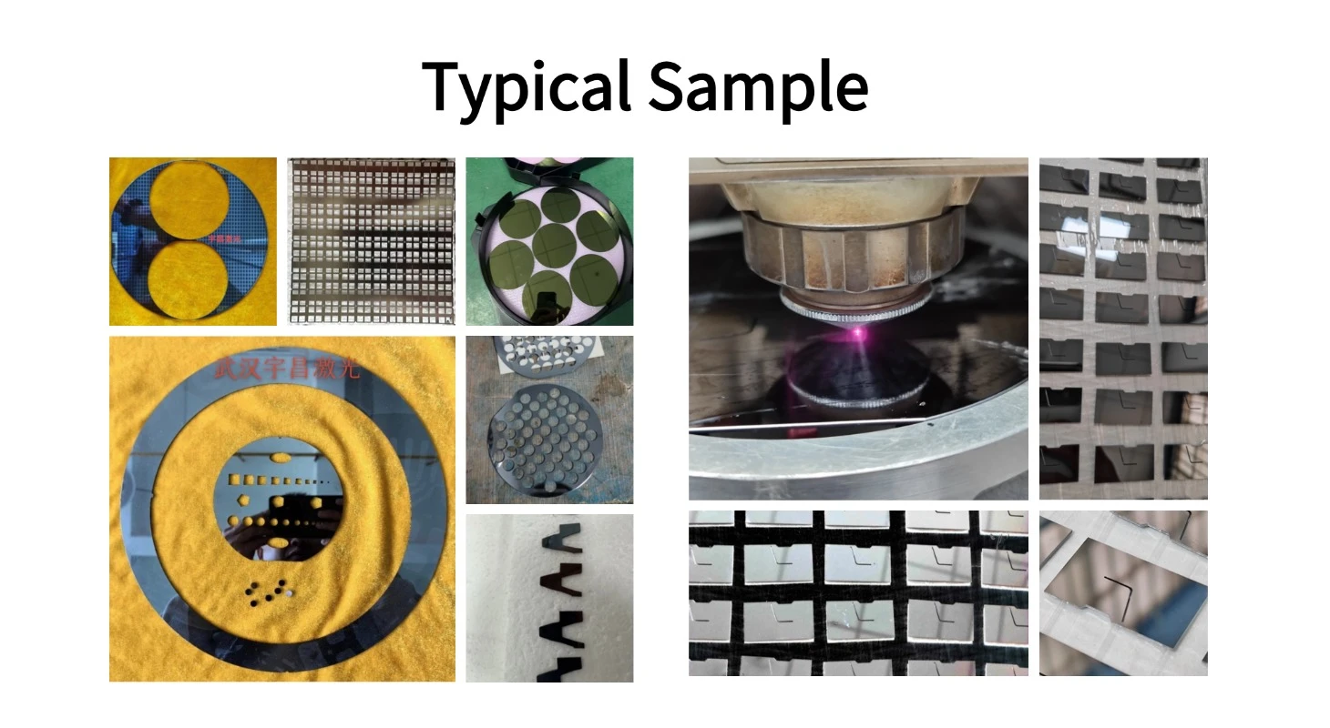
Laser dicing uses a focused laser beam to process predefined dicing streets between semiconductor devices on a wafer.
A typical process includes:
Wafer Loading → Vision Alignment → Laser Processing → Separation → Inspection
Depending on the process, the laser may:
- Remove material directly through laser ablation
- Create a narrow groove or scribe path
- Modify material internally for controlled separation
- Process selected contours or non-linear geometries
The final objective is not simply to separate the wafer. A practical dicing process must balance kerf width, chipping, cracking, thermal effects, dimensional accuracy, processing speed, and die edge quality.
For semiconductor applications, the selected dicing method also needs to account for structures located within or around the dicing streets, including metallization and other device-related features.
How Does Laser Dicing Work?
A laser dicing system combines the laser source with precision optics, motion control, vision alignment, wafer fixturing, and process-control software.
1. Wafer Loading: The wafer is positioned on a suitable chuck or fixture to maintain stable positioning during processing.
2. Vision Alignment: A vision system identifies wafer features and aligns the programmed dicing paths with the actual wafer position.
3. Laser Focusing:The optical system focuses the laser beam at the required processing position. Focus depth and beam characteristics depend on the wafer material and selected process.
4. Laser Processing:The laser follows the programmed dicing streets to remove or modify material.
5. Separation:For direct laser ablation, the laser removes material along the cutting path. For suitable stealth dicing processes, the laser creates an internal modified layer that acts as a starting point for controlled fracture, followed by a separate wafer separation step.
6. Inspection:The processed wafer or individual dies can then be inspected for edge quality, chipping, cracks, kerf width, dimensional accuracy, and other application-specific requirements.
What Are the Main Wafer Dicing Methods?
Different wafer materials and device structures require different singulation approaches.
| Wafer Dicing Method | Basic Principle | Main Considerations |
| Mechanical Blade Dicing | A rotating blade mechanically removes material | Tool wear, mechanical stress, kerf and chipping |
| Scribe & Break | A defined scribe line is followed by controlled fracture | Material properties and fracture control |
| Laser Ablation Dicing | A focused laser directly removes material | Thermal effects, debris and kerf |
| Laser Stealth Dicing | A laser creates an internal modified layer for separation | Material properties, optical transmission and separation process |
| Plasma Dicing | Plasma etches predefined wafer areas | Process complexity and equipment requirements |
There is no single wafer dicing method suitable for every application. Material, thickness, wafer structure, dicing street design, required edge quality and production requirements all influence the appropriate process.
Laser Dicing of Silicon Wafers
Silicon wafer laser cutting is an important application of laser-based wafer singulation. For silicon wafers, the appropriate process depends on factors such as:
- Wafer thickness
- Crystal orientation
- Dicing street width
- Device structure
- Required kerf
- Edge quality
- Processing speed
- Separation method
Laser Dicing for Semiconductors
Laser dicing can be considered for a range of semiconductor and semiconductor-related materials, but the process window varies significantly between materials.
Silicon
Silicon wafers can be processed using direct laser dicing or suitable internal-modification processes, depending on wafer structure and requirements.
Silicon Carbide (SiC)
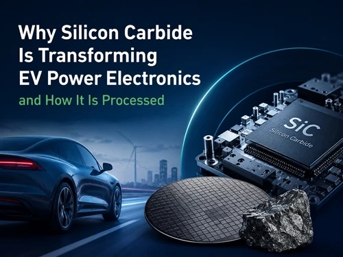
SiC is a hard, brittle material used extensively in power semiconductor applications. Its material properties make dicing particularly sensitive to chipping, cracking and thermal effects. Laser-based approaches, including ultrafast and stealth-type processes, are being investigated and developed for SiC wafer singulation.
Sapphire
Sapphire is a hard and brittle material used in optoelectronic and semiconductor-related applications. Laser processing can be considered when conventional mechanical processing presents limitations.
Ceramic Materials
Advanced ceramics such as Al₂O₃, AlN, Si₃N₄ and SiC are also processed for semiconductor packaging, power electronics and electronic components.
Laser Dicing of Ceramic Wafers and Substrates
Laser dicing is not limited to semiconductor wafers.
Ceramic materials used in electronic and semiconductor applications can also require precision cutting, singulation, slotting, or contour processing.
Typical materials include:
- Alumina (Al₂O₃)
- Aluminum Nitride (AlN)
- Silicon Nitride (Si₃N₄)
- Silicon Carbide (SiC)
- LTCC and HTCC
- DBC, DPC and AMB ceramic substrates
For these applications, the suitable laser source depends on the material composition, thickness, geometry, thermal sensitivity and required edge quality.
Dicing ceramic materials should therefore be evaluated as a specific material-processing application rather than treated in exactly the same way as silicon wafer dicing.
A laser dicing system is an integrated processing platform rather than simply a laser mounted on a machine.
A typical system includes:
Laser Source:The laser wavelength, pulse duration, power and repetition rate are selected according to the material and process requirements.
Beam Delivery and Optics:The optical system controls beam delivery, focusing and spot characteristics.
Precision Motion Stage:The motion system follows the programmed dicing paths while maintaining the required positioning accuracy.
Vision Alignment:CCD or machine vision can be used to identify wafer features and align the processing path.
Wafer Fixture:A suitable chuck or fixture keeps the wafer stable during laser processing.
Process Control:Control software manages laser parameters, motion paths, processing sequences and other machine functions.
For production applications, these components need to work together as a complete process system.
How to Choose a Laser Dicing System
When selecting a laser dicing system, the first consideration should be the actual material and processing requirement.
1. Wafer Material
2. Wafer Thickness
3. Required Edge Quality
4. Wafer Size and Geometry
5. Production Requirements
6. Automation
Key Factors Affecting Wafer Dicing Quality
Several factors influence the final quality of semiconductor wafer dicing.
Kerf Width
A narrower processing path can reduce material loss and may provide more usable wafer area, depending on the application.
Chipping
Excessive edge chipping can affect subsequent assembly and device reliability requirements.
Cracking
Cracks extending beyond the intended dicing region can reduce die quality.
Thermal Effects
Laser parameters must be controlled to limit unwanted heat accumulation and thermal damage.
Debris
Direct laser ablation can generate particles or redeposited material, making process control and extraction important.
Dimensional Accuracy
Laser positioning, motion accuracy, vision alignment and material response all contribute to final cutting accuracy.
Semiconductor Dicing Applications
Laser-based dicing can be considered for applications including:
- Power semiconductors: SiC and GaN devices
- MEMS and sensors: precision wafer singulation
- RF and compound semiconductors: GaN and GaAs-related devices
- Optoelectronics: selected semiconductor and sapphire applications
- Advanced packaging: ceramic substrates and package components
- Electronic ceramics: alumina, AlN, Si₃N₄ and SiC components
The actual processing method should be selected according to the material and device structure.
YCLaser Dicing Solutions
YCLaser develops laser processing systems for semiconductor materials, advanced ceramics and other hard and brittle materials.
Learn more about us
Depending on the material, thickness and processing requirements, available configurations can include:
Customized laser configurations
Systems can be configured with precision motion platforms, vision alignment, customized fixtures, and automation options according to application requirements.
For the fastest response, please contactus via WhatsApp.(Click the WhatsApp button on the screen)